(China (Mainland))

Product Summary
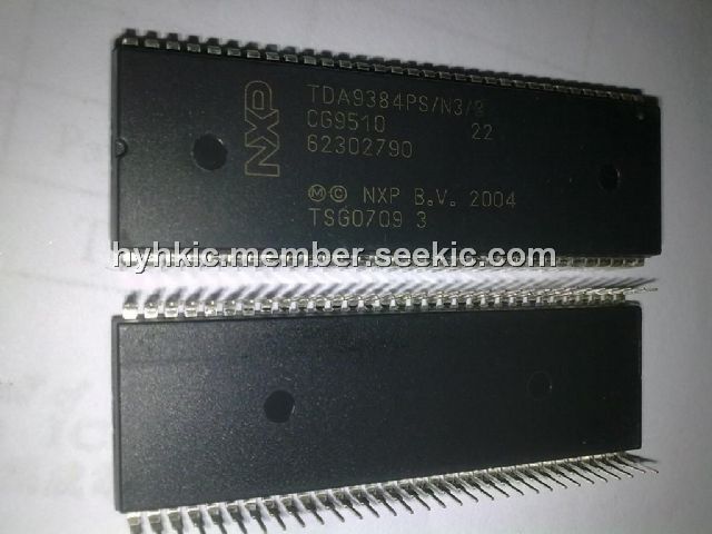
The TDA9384PS/N3/3 is an input processor for High-end television receivers. The TDA9384PS/N3/3 contains the following functions: Multistandard IF amplifier with PLL demodulator, QSS-IF amplifier and AM sound demodulator, CVBS and Y/C switch with various inputs and outputs, Multistandard colour decoder which can also decode the PALplus helper signal, Integrated baseband delay line (64 ms), Sync processor which generates the horizontal and vertical drive pulses for the feature box (100 Hz applications) or display processor (50 Hz applications). The supply voltage for the TDA9384PS/N3/3 is 8 V.
Parametrics
TDA9384PS/N3/3 absolute maximum ratings: (1)VP supply voltage(pins VP1 and VP2): 7.2, 8.0, 8.8 V; (2)IP supply current(pins VP1 and VP2): 120, 140 mA; (3)Ptot total power dissipation: 960mW.
Features
TDA9384PS/N3/3 features: (1) Multistandard Vision IF (VIF)circuit with Phase-Locked Loop (PLL)demodulator; (2) Sound IF (SIF)amplifier with separate input for single reference Quasi Split Sound (QSS)mode and separate Automatic Gain Control (AGC)circuit; (3) AM demodulator without extra reference circuit; (4) Switchable group delay correction circuit which can be used to compensate the group delay pre-correction of the B/G TV standard in multistandard TV receivers; (5) Several (I2C-bus controlled)switch outputs which can be used to switch external circuits such as sound traps, etc.; (6) Flexible source selection circuit with 2 external CVBS inputs, 2 Luminance (Y)and Chrominance (C); (7)(or additional CVBS)inputs and 2 independently switchable outputs; (8) Comb filter interface with CVBS output and Y/C input; (9) Integrated chrominance trap circuit; (10) Integrated luminance delay line with adjustable delay time; (11) Integrated chrominance band-pass filter with switchable centre frequency; (12) Multistandard colour decoder with 4 separate pins for crystal connection and automatic search system; (13) PALplus helper demodulator; (14) Possible blanking of the helper signals for PALplus and EDTV-2; (15) Internal baseband delay line.
Diagrams
 |
 TDA9102C |
Other |
|
Data Sheet |
Negotiable |
|
||||
|
TDA9102F |
Other |
|
Data Sheet |
Negotiable |
|
||||
|
TDA9102T |
Other |
|
Data Sheet |
Negotiable |
|
||||
|
TDA9103 |
Other |
|
Data Sheet |
Negotiable |
|
||||
|
TDA9105 |
Other |
|
Data Sheet |
Negotiable |
|
||||
|
TDA9105A |
Other |
|
Data Sheet |
Negotiable |
|
||||