(China (Mainland))

Product Summary
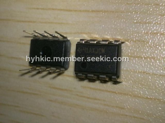
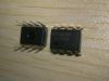
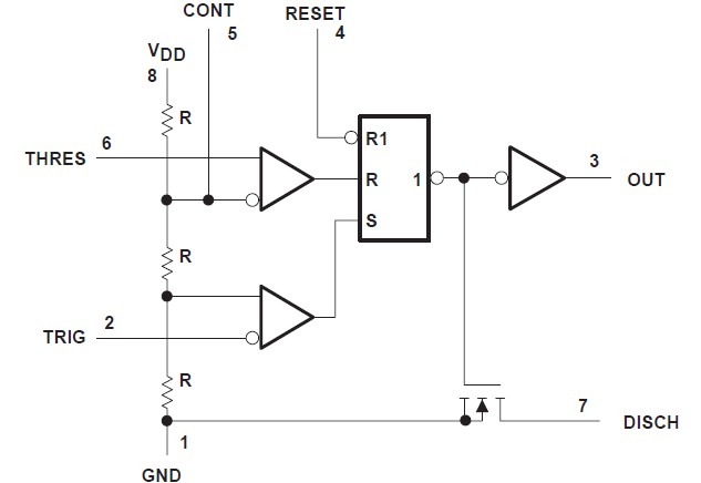
The TLC555IP is a LinCMOSE TIMER. Like the NE555, the TLC555IP has a trigger level equal to approximately one-third of the supply voltage and a threshold level equal to approximately two-thirds of the supply voltage. These levels can be altered by use of the control voltage terminal (CONT). When the trigger input (TRIG) falls below the trigger level, the flip-flop is set and the output goes high. If TRIG is above the trigger level and the threshold input (THRES) is above the threshold level, the flip-flop is reset and the output is low. The reset input (RESET) can override all other inputs and can be used to initiate a new timing cycle. If RESET is low, the flip-flop is reset and the output is low. Whenever the output is low, a low-impedance path is provided between the discharge terminal (DISCH) and GND. All unused inputs should be tied to an appropriate logic level to prevent false triggering. While the CMOS output is capable of sinking over 100 mA and sourcing over 10 mA, the TLC555IP exhibits greatly reduced supply-current spikes during output transitions. This minimizes the need for the large decoupling capacitors required by the NE555.
Parametrics
TLC555IP absolute maximum ratings: (1)Supply voltage, VDD (see Note 1): 18 V; (2)Input voltage range, VI (any input): -0.3 to VDD; (3)Sink current, discharge or output: 150 mA; (4)Source current, output, IO: 15 mA; (5)Continuous total power dissipation: See Dissipation Rating Table; (6)Storage temperature range: -65°C to 150°C; (7)Case temperature for 60 seconds: FK package: 260°C; (8)Lead temperature 1,6 mm (1/16 inch)from case for 60 seconds: JG package: 300°C; (9)Lead temperature 1,6 mm (1/16 inch)from case for 10 seconds: D, DB, P, or PW package: 260°C.
Features
TLC555IP features: (1)Very Low Power Consumption: 1 mW Typ at VDD = 5 V; (2)Capable of Operation in Astable Mode; (3)CMOS Output Capable of Swinging Rail to Rail; (4)High Output-Current Capability: Sink 100 mA Typ, Source 10 mA Typ; (5)Output Fully Compatible With CMOS, TTL, and MOS; (6)Low Supply Current Reduces Spikes During Output Transitions; (7)Single-Supply Operation From 2 V to 15 V; (8)Functionally Interchangeable With the NE555; Has Same Pinout; (9)ESD Protection Exceeds 2000 V Per MIL-STD-883C, Method 3015.2; (10)Available in Q-Temp Automotive: High Reliability Automotive Applications, Configuration Control/Print Support, Qualification to Automotive Standards.
Diagrams
| Image | Part No | Mfg | Description |  |
Pricing (USD) |
Quantity | ||||||||||||
|---|---|---|---|---|---|---|---|---|---|---|---|---|---|---|---|---|---|---|
 |
 TLC555IPE4 |
Texas Instruments |
Timers & Support Products LOW POWER TIMER |
Data Sheet |
|
|
||||||||||||
|
TLC555IP |
Texas Instruments |
Timers & Support Products CMOS |
Data Sheet |
|
|
||||||||||||